 MyVoice home [NL]
|
LPC2xxx board
Support for different QuickStart boards
The LPC2106 (RS232), LPC213x and LPC214x QSB modules must fit on the board.
The LPC2106 modules have 2x20 pins with a 600 mil spacing, the LPC213x and 214x contain 2 blocks of 2x16 pins with 1100 mil spacing. Both modules can therefor be placed at the same location on the development board. In this way only a 2106 or 213x board can be placed.
Since the LPC2106 board does not contain an RS232 buffer, the development board must contain an RS232 tranceiver. Jumpers will be placed to switch the tranceiver on the development board to either the LPC2106 or 213x pin headers. The RTS and DTR signals will be used for automatic bootloader activation.
All IO pins (except the P0.0 and P0.1 pins for UART0) will be connected to both QSB modules.
|
On board IO options
The development board will contain a number of standard IO devices:
- UART1 may be connected to a second RS232 connector. This is jumper configurable (combines with the high intensity LEDs).
- LCD connected to the I2C bus
The LCD contrast voltage (negative voltage) is connected to P0.21/PWM5 via a jumper.
The LCD backlight (LEDs or LED foil) can be connected to P0.7/PWM2 or P0.8/PWM4
Pull up resistors on the I2C bus can be connected using jumpers for the LPC2106 board (the LPC213x board has these pull up resistors on board)
- 4 keys connected to P0.17 .. P0.20 with the common rail to P0.16/EINT0
This makes it possible to use the EINT0 pin as a wakeup event from power down/idle mode via a keypress
- TIL311 and DL1414 displays are connected to P0.24 .. P0.30 (datalines), P0.31 is used to select the latch in the TIL311 or DL1414 and P0.22/0.23 are connected to A0/1 of the DL1414
These displays are primarily used to show program status during debugging, due to power consumption of the LED displays there will not be used in battery powered applications
- An SD/MMC bay will be connected to the SPI channel, chip select of the SD card is connected to SSEL0
- High intensity LEDs, driven by MOSFET transistors will be connected to P0.8/PWM4 and P0.9/PWM6
- 4 LEDs are connected to P0.10..P0.13 in such a way that the LED is on if a '1' is written to the corresponsing pin
- All IO pins of P1 are available on a pin header (together with power signals)
Unused- and some of the pins from P0 (maybe I should say all) will also be available at a pin header.
- A PCF8574 I2C IO expander is fitted with 4 LEDs and 4 keys, the interrupt line of the IO expander is connected to P0.16/EINT0 that is also used for the directly connected keys.
- For the keys connected to the PCF8574 types with an LCD in the key will be used. These LCDs are controlled by PCF8576 controllers.
Few of the requirements may look strange, I always like to have all pins available for external IO but I'm not sure if that's manageble with my only options of creating double layer PCBs with manual via soldering ...
|
JTAG
The JTAG of the LPC213x board is connected to a 20 pins header, a jumper placed on the RTCK line will enable the JTAG interface.
I am not yet sure what to do with the JTAG of the LPC2106 board, it may be cross connected with the JTAG of the LPC213x board.
|
Power supply
The LPC213x/214x board may be powered by USB, in that case the whole board may be powered via the USB.
Current drawn by the different components may be measured via jumpers placed in the power lines. Current (on the 5V line) to the QSB module can only be measured if the module is powered from the main development board. External (to the QSB module) powered components that require 3.3V can be switched of. The RS232 tranceivers and I2C components are controlled by different jumper sets.
The TIL311 and DL1414 displays will be connected to the 5V power, both modules do work with a 3.3V IO voltage level. Both displays are socketed so they can be removed if power measurement without these displays is needed.
| |
Photo's and datasheets
|
|
|
The key with encapsulated LCD. Each key contains one PCF8576 LCD controller. The LCD contains 12x8 pixels using all 4 backplanes of the LCD controller |
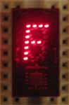
The TIL311 is the well known hexadecimal display seen on a lot of older development boards, I still have some once bought at a surplus store. |
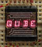
From HP, the DL1414 is famous for its abilities to provide text output (when introduced). Nowadays more expensive than an LCD but I still have some bought at a surplus store. |
- The SD/MMC connector, available in different footprints. The Physical Layer specification of the SD card Association is not available without licensing but the simplified version is available at their website. An article in Circuit Cellar #176 "Portable FAT library for MCU applications" shows how to control the SD card.
- PCF8574T - 8 bit IO expander with interrupt control.
- MAX3232 - RS232 tranceiver for 2 transmit and 2 receive lines (for UART0 & 1 Rx/Tx control).
- BC847C & BAW56 - General purpose NPN transistor and hish speed diode as used in the RTS/DTR handling for the bootloader in combination with the LPC21ISP program.
- IRF540NS - N channel MOSFET with Id=33A in D2Pak housing for real power applications
IRF7403 - N channel MOSFET in SO-8 Id=8.6A, still big enough for controlling Luxeon LEDs in my end application.
Both MOSFETs are selected on a low Vgs threshold voltage and a low Ron. The Ron is specified at Vgs=10V, at lower voltages Ron will raise and the max. continuous Id will drop. On the development board only the IRF7403 will be used.
|
Schematics and board layout
Are not yet available.
One of the constraints of the board layout will be that all connectors will be placed at the outer edges of the board (this includes the connectors on the QSB modules). Keys have to be placed at the lowed edge (easy to reach) and a reset key somewhere near the QSB module, IO keys will be Digitast type and the reset key a low profile key. Displays and LEDs will be placed next to the displays, except the high intensity LEDs (don't want to blind my vision ...)
|
|
|
|